Sunday, August 14, 2005
This Day:

NanoTubes are traditionally cylindrical Carbon molecules with properties that make them potentially useful in extremely small scale electronic and mechanical applications. They exhibit unusual strength and unique electrical properties, and are efficient conductors of heat.
Scientists Prab Bandaru and colleagues at the UC San Diego, and Apparao Rao, of Clemson University, have now crafted such nanotubes in the shape of a 'Y', which could revolutionise the computer industry, as the nanotubes are easily made and act as remarkably efficient electronic transistors:).
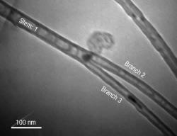
'Y' transistor (Courtesy: New Scientist)
Experiments show that applying a voltage to the stem of the Y precisely controls the flow of electrons through the other two branches. The switching capacity of these nanostructures is, in comparable to that of today's silicon transistors.
But whereas current silicon transistors have been shrunk to around 100 nanometres, the Y-shaped nanotubes measure just tens of nanometres in size. Eventually, they could even be shrunk to just a few nanometres, the researchers suggest:D:D.

(Hide) (Show)

9 Comments:

At August 17, 2005 10:01 AM, Blogger Wayne Smallman said...
I don't see any real end to the possibilities of nanotubes.

For one, there has to be no end to medical applications alone...
 
At August 17, 2005 10:06 AM, Blogger Sray said...
This is going to be the century of nanotubes :).
 
At August 17, 2005 9:04 PM, Blogger Unknown said...
To revolutionize the 'industry', just being able to make nanotube transistors wont be enuf. WE will need some cheap, efficient and non-time-consuming techniques to mass produce them, like we have photolithography for today's chips
 
At August 17, 2005 9:47 PM, Blogger Sray said...
Yes! And it seems that this 'Y' nanotube can be mass-produced and chips can be made by etching nano-circuits with that.
 
At August 17, 2005 10:34 PM, Blogger Unknown said...
Wow! Thats news!

I'll be waiting for u to post on the mass production technique
 
At August 18, 2005 3:45 AM, Blogger Sray said...
:):).. one really cute way that is being developed is to etch the substrate using laser, treat it with some chemical, and then dip it in a solution containing the tubes. The tubes automatically attach to the chemical-filled etches, and the rest of the chemical is then washed away to get the circuit!
 
At August 18, 2005 7:51 AM, Blogger Unknown said...
Wow! ANy links to some more setails? It seems to be quite interesting.
 
At August 18, 2005 1:58 PM, Blogger Sray said...
I think I had a post on this a couple of weeks back :-? :).
 
At August 18, 2005 11:07 PM, Blogger Unknown said...
Alright, I'll have to hunt the archives
 

Post a Comment